

Laptops may have made hand-writing notes a thing of the past, but the pencil — or at least pencil lead — is making a comeback, as UA researchers are developing ways to use pencil lead as a conductor in electronics.
Brian LeRoy, an assistant professor in the physics department, along with Matthew Yankowitz and Daniel Cormode, two physics graduate students, published their findings in the science journal Nature Physics.
Graphite, which is used to make pencil lead, can be broken down into one atomic layer and then becomes graphene, Yankowitz said. “People are interested in graphene because they think that it can replace silicon in next-generation electronics,” he added.
The layers themselves are microscopically thin, hexagonal lattices, Cormode said. If a sheet of paper were as tall as a desk, a layer of graphene would be thinner than an actual sheet of paper sitting on the desk.
Silicon has long served as the primary electronic conductor for products in the technology market like today’s computers, and, as a metal, works as an on and off switch. This allows electrons to conduct through the device when turned on, immobilizing them when turned off.
LeRoy and fellow researchers who specialize in studying the electronic properties of certain materials are looking to replace silicon with graphene, which tends to be more efficient at moving the electrons. Silicon is a very resistant metal by nature, Cormode said, and produces heat. In turn, devices must power a coolant source, like fans. Graphene works as a less-resistant conductor, which will not only move the electrons through the device faster, but also avoid the heat production that silicon’s resistance causes.
After determining graphene’s electronic properties, the trick was controlling the electrons in the material. This is done by placing the graphene lattice on boron nitride, a material that is equivalent in structure to graphite. Because both materials are structured in hexagonal shapes, placing graphite’s lattice onto the lattice created by boron nitride allows researchers, through relativistic quantum mechanics, to control the flow of electrons through the graphene.
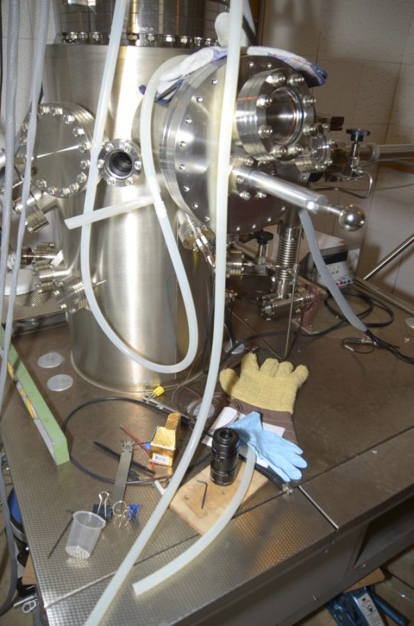
Using a scanning tunneling microscope, LeRoy and his colleagues can monitor the positioning of the graphene. The slightest movement of the lattice can change the current of the electrons drastically.
The difficulty with this process, Yankowitz said, is its counterintuitiveness. Placing the lattices together and rotating them creates openings, but the openings don’t necessarily allow the electrons to go through.
“There’s a weird thing in graphene due to relativistic quantum mechanics that says that no matter how big of a wall that you put in front of them (the electrons), they’ll just keep going through anyway,” Yankowitz said.
This is a problem when making electronics, he said, as the electrons will continue to move through the material even when the device is switched off.
With the research still in the early exploratory process, LeRoy said graphene’s implementation into electronics is still well into the future.
“I would say there’s probably limited applications where you may want to use it,” he added. “I doubt you’re ever, at least in the next 15 years, going to buy a computer that has its CPU replaced with some graphene, but maybe your cellphone will have some high-speed transistor in it that’s made out of graphene for a very specific application.”